

Intel recently hosted IFS Direct Connect 2024, an event showcasing the capabilities of Intel’s Foundry business. CEO Pat Gelsinger presented a new vision for the company, with an extended roadmap of technologies and architectures. We review the announcements and the implications for the future of Intel and the chip business.
In what has become a series of promotional events to sell the virtues of the 2021 IDM (Integrated Device Manufacturing) 2.0 strategy, Intel recently held a media event to publicise its foundry business. CEO Pat Gelsinger announced a reorganisation of the company into two new legal entities. Intel Foundry will operate as an independent business, developing the manufacturing capability, while Intel Products will continue the design and production of processors and associated solutions.
Intel Foundry
Intel has bet big on the idea of a separate foundry business as a way to rejuvenate the fortunes of the company. IDM 2.0, announced in March 2021, set the framework for new fabrication plants (fabs) in Arizona, followed by investments in similar manufacturing capabilities in Europe.
Gelsinger wants to become the world’s manufacturing facility, with the goal of being number 2 in the industry by 2030. The core of this strategy is the evolving Intel Foundry business, initially a division and now a separate legal entity that would remain wholly owned by Intel.
The foundry business is underpinned by three principles. The first is to develop a world-class foundry offering. This means being the first to deliver the manufacturing capability for new process nodes while introducing new techniques and technologies to the production of chips.
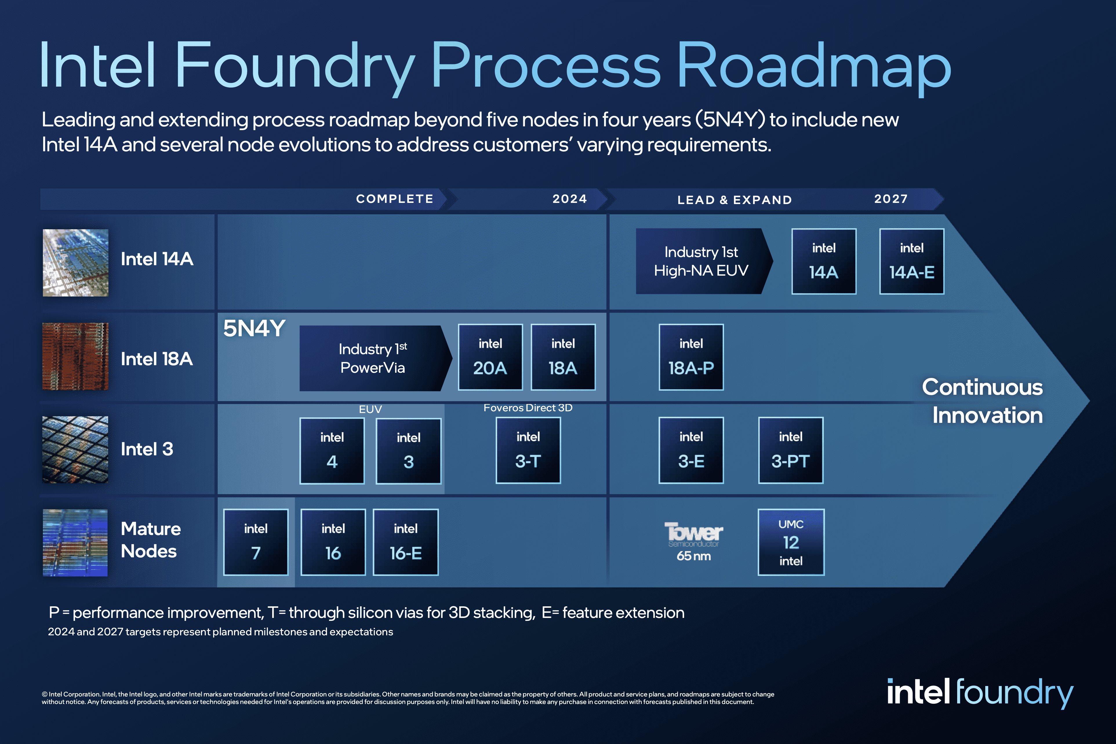
Since IDM 2.0 was announced, Intel has been moving forward with 5N4Y, otherwise known as 5 nodes in 4 years. These are:
- Intel 7 – previously known as Intel 10nm Enhanced SuperFin (10ESF) and used to deliver the Alder Lake and Raptor Lake processors (12th and 13th generation Core processors, respectively).
- Intel 4 – a 7nm process being used to deliver the 14th generation Core processors (Meteor Lake) and the first to use EUV (extreme ultraviolet) lithography.
- Intel 3 – a 5nm process (we think) that will also exploit EUV and be used to deliver Sierra Forest.
- Intel 20A – used to deliver Arrow Lake, the successor to Meteor Lake, with products expected in 2024. The designation of dimensions changes to use angstroms (where 10 angstroms = 1nm), so this is potentially a 2nm process.
- Intel 18A – used to deliver Xeon processors built on the Clearwater Forest design and Lunar Lake Core processors. This node is potentially a 1.8nm or 18-angstrom process.
So far, it looks like Intel will be on schedule to deliver the promise of 5N4Y. At Direct Connect, Gelsinger took the opportunity to announce 14A, the next process step on the roadmap that extends past the final 5N4Y process. 14A will be built using High-NA EUV technology, of which ASML is the sole manufacturer and Intel the first customer to receive this $380 million monolith (TSMC is potentially delaying to 2030 before adoption).
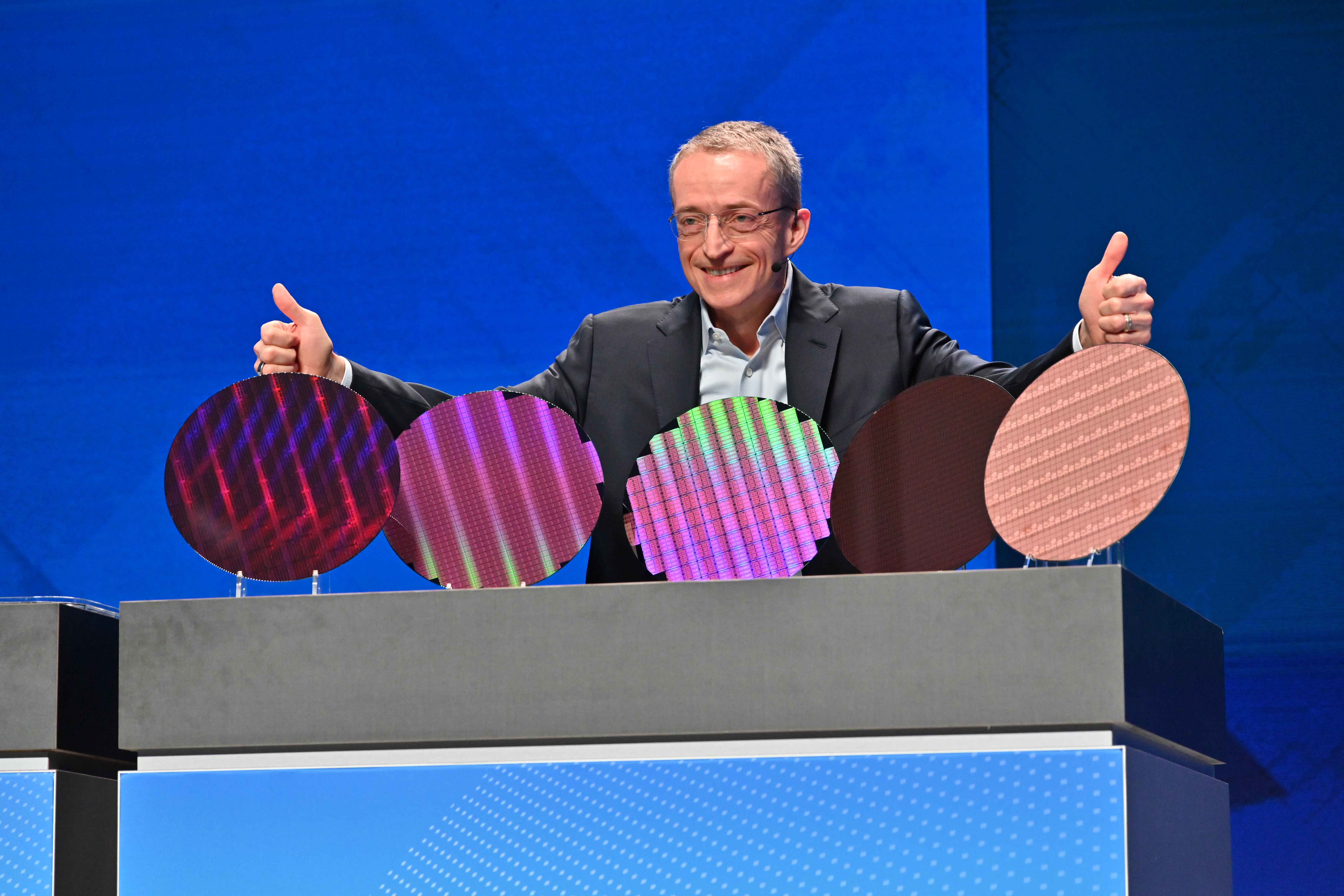
Existing process capabilities will also be extended (see figure 1), with feature extensions and performance improvement capabilities reminiscent of the old “tick-tock” architectural roadmap.
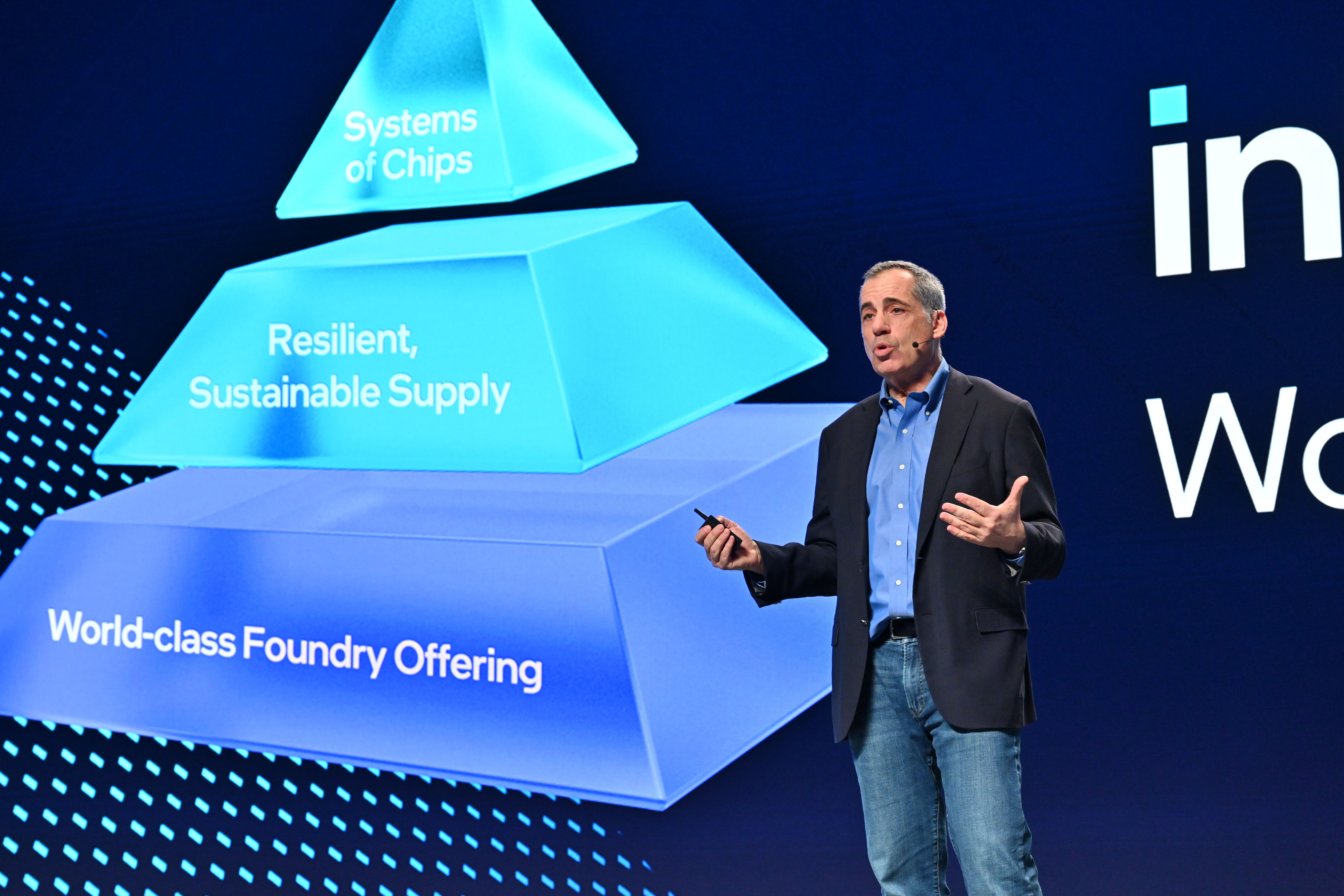
The second principle is to build a sustainable and resilient foundry business. Sustainability is seen as key to delivering the volume of chips required to drive forward the adoption of AI, while resiliency reflects the need for strong supply chains and reduced dependency on Asia. Gelsinger wants manufacturing to reach 50/50 across US/Europe and Asia compared to 20/80 today.
The third principle is to build systems of chips. It’s clear that SoC packaging is the route forward for the development of modern processors. As SVP and GM for the Intel Foundry Services business, Stuart Pann highlighted onstage, it isn’t possible for all on-die components to be reduced in process size at the same rate. Therefore, as Gordon Moore highlighted back in 1965, packaging may be a more efficient process.
To that end, Intel has developed new packaging techniques like Foveros 3D and EMIB (embedded multi-die interconnect bridge), glass substrates and efficient power delivery with PowerVia, all of which are existing technologies we’ve previously discussed.
The Architects View®
Pat Gelsinger has bet the business on the success of the foundry strategy. Separating Intel Foundry as a discrete business with an independent profit & loss account is essential if the company is to attract the businesses name checked during Gelsinger’s presentation. These included NVIDIA, AMD, Qualcomm, and Google, while Microsoft got an honorary mention with a presentation from CEO Satya Nadella. Microsoft and Intel are collaborating on an, as yet unspecified, device built on the 18A process. During the presentation from Stuart Pann, Arm CEO Rene Haas appeared onstage to discuss a collaboration initiative between the two companies. It’s clear that Intel is serious about making the foundry business work, even with its most fierce competitors.
What does that say about the remainder of Intel, the parts that fall under Intel Products? As we’ve discussed before, the processor business is highly competitive, with both AMD and Arm increasing their share in enterprise and consumer markets. The big money is (currently) headed into GPUs, where Intel isn’t as competitive.
Focusing on manufacturing gives Intel two benefits. First, the US government will subsidise the building of infrastructure as part of the Chips Act (and a rumoured Chips Act 2, if the discussion with US Secretary of Commerce, Gina Raimondo is to be believed), and this money would be ring-fenced in the Foundry legal entity.
If Intel can capture a decent percentage of the manufacturing market (currently $15 billion of prospective orders are already in place), then this provides breathing space to review the technology strategy within Intel Products.
The second benefit is clearly that Intel wins manufacturing revenue, even as it loses out on product sales. One big caveat here is that IFS currently represents only 1.7% of Intel’s revenue (FY2023 data), so there’s a long way to go for IFS to be impactful on the top and bottom line of Intel Corporation.
Intel already makes SKU-specific products for the hyper-scalers, but increasingly we are seeing those companies moving to create bespoke in-house architectures. Today this means Arm-based systems, but in the future could encompass RISC-V. The greatest risk for Intel is the fragmentation of the processor market and a reduced dependency on the x86 architecture. Therefore, even if Intel Foundry is a success, renewed focus on products is still essential.
In that respect, Intel Foundry is an each-way bet. One way Intel wins by manufacturing the hardware, the other it wins by designing and manufacturing it. This transformation is going to take a decade to play out, with many twists and turns still to come. Whether the Foundry gamble will be a success remains to be seen.
Copyright (c) 2007-2024 – Post #ce38 – Brookend Limited, first published on https://www.architecting.it/blog, do not reproduce without permission. Images copyright Intel.